Welcome Guest
  |   0 items in your shopping cart
 

BROWSE BY STANDARDS

BROWSE BY CATEGORY

***
 
 
Join our mailing list to recieve newsletters
 

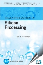
Characterization in Silicon Processing

Send to friend
 
Title: Characterization in Silicon Processing
Author: Yale E. Strausser
ISBN: 1606501097 / 9781606501092
Format: Hard Cover
Pages: 240
Publisher: Momentum Press
Year: 2009
Availability: Out of Stock
     
 
  • Description
  • Contents

With a focus on the use of materials characterization techniques for silicon-based semiconductors, this volume in the Materials Characterization series focuses on the process flow of silicon wafer manufacture where materials properties, processing and associated problems are brought to the fore. The book is organized by the types of materials commonly associated with integrated silicon semiconductor circuits and the typical processes involved for each such material, including deposition, thermal treatment, and lithography. Readers will find features such as:

  • The essential processes of Silicon Epitaxial Growth
  • Coverage of Polysilicon Conductors, Silicides, Aluminum- and Copper-based Conductors, Tungsten-based Conductors
  • Concise summaries of major characterization technologies for silicon and related semiconductor materials, including Auger Electron Spectroscopy, Energy-Dispersive X-Ray Spectroscopy, Neutron Activation Analysis and Raman Spectroscopy

Preface to the Reissue of the Materials Characterization Series
Preface to Series
Preface to the Reissue of Characterization in Silicon Processing
Preface
Contributors

Chapter 1 : Application of Materials Characterization Techniques to Silicon Epitaxial Growth
Chapter 2 : Polysilicon Conductors
Chapter 3 : Silicides
Chapter 4 : Aluminum-And Copper-Based Conductors
Chapter 5 : Tungsten-Based Conductors
Chapter 6 : Barrier Films

Appendix : Technique Summaries
1 : Auger Electron Spectroscopy (AES)
2 : Ballistic Electron Emission Microscopy (BEEM)
3 : Capacitance-Voltage (C-V) Measurements
4 : Deep Level Transient Spectroscopy (DLTS)
5 : Dynamic Secondary Ion Mass Spectrometry (Dynamic SIMS)
6 : Electron Beam Induced Current (EBIC) Microscopy
7 : Energy-Dispersive X-Ray Spectroscopy (EDS)
8 : Focused Ion Beams (FIBs)
9 : Fourier Transform Infrared Spectroscopy (FTIR)
10 : Hall Effect Resistivity Measurements
11 : Inductively Coupled Plasma Mass Spectrometry (ICPMS)
12 : Light Microscopy
13 : Low-Energy Electron Diffraction (LEED)
14 : Neutron Activation Analysis (NAA)
15 : Optical Scatterometry
16 : Photoluminescence (PL)
17 : Raman Spectroscopy
18 : Reflection High-Energy Electron Diffraction (RHEED)
19 : Rutherford Backscattering Spectrometry (RBS)
20 : Scanning Electron Microscopy (SEM)
21 : Scanning Transmission Electron Microscopy (STEM)
22 : Scanning Tunneling Microscopy and Scanning Force Microscopy (STM and SFM)
23 : Sheet Resistance and the Four Point Probe
24 : Spreading Resistance Analysis (SRA)
25 : Static Secondary Ion Mass Spectrometry (Static SIMS)
26 : Surface Roughness: Measurement, Formation by Sputtering Impact on Depth Profiling
27 : Total Reflection X-Ray Fluorescence Analysis (TXRF)
28 : Transmission Electron Microscopy (TEM)
29 : Variable-Angle Spectroscopic Ellipsometry (VASE)
30 : X-Ray Diffraction (XRD)
31 : X-Ray Fluorescence (XRF)
32 : X-Ray-Photoelectron Spectroscopy (XPS)

Index


About Us | Contact us
loading...
This page was created in 0.6451621055603 seconds