Welcome Guest
  |   0 items in your shopping cart
 

BROWSE BY STANDARDS

BROWSE BY CATEGORY

***
 
 
Join our mailing list to recieve newsletters
 

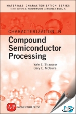
Characterization in Compound Semiconductor Processing

Send to friend
 
Title: Characterization in Compound Semiconductor Processing
Author: Gary E. McGuire, Yale E. Strausser
ISBN: 1606500414 / 9781606500415
Format: Hard Cover
Pages: 200
Publisher: Momentum Press
Year: 2009
Availability: Out of Stock
     
 
  • Description
  • Contents

Compound semiconductors such as Gallium Arsenide, Gallium Aluminum Arsenide, and Indium Phosphide are often difficult to characterize and present a variety of challenges from substrate preparation, to epitaxial growth to dielectric film deposition to dopant introduction.

This book reviews the common classes of compound semiconductors, their physical, optical and electrical properties and the various types of methods used for characterizing them when analyzing for defects and application problems.

The book features:

  • Characterization of III-V Thin Films for Electronic and Optical applications
  • Characterization of Dielectric Insulating Film layers
  • A Special case study on Deep Level Transient Spectroscopy on GaAs
  • Concise summaries of major characterization technologies for compound semiconductor materials, including Auger Electron Spectroscopy, Ballistic Electron Emission Microscopy, Energy-Dispersive X-Ray Spectroscopy, Neutron Activation Analysis and Raman Spectroscopy

Preface to the Reissue of the Materials Characterization Series
Preface to Series
Preface to the Reissue of Characterization of Compound Semiconductor Processing
Preface
Contributors

Chapter 1 : Characterization of III-V Thin Films for Electronic Devices
Chapter 2 : III-V Compound Semiconductor Films for Optical Applications
Chapter 3 : Contacts
Chapter 4 : Dielectric Insulating Layers
Chapter 5 : Other Compound Semiconductor Films
Chapter 6 : Deep Level Transient Spectroscopy : A Case Study On GaAs

Appendix: Technique Summaries
1 : Auger Electron Spectroscopy (AES)
2 : Ballistic Electron Emission Microscopy (BEEM)
3 : Capacitance-Voltage (C-V) Measurements
4 : Deep Level Transient Spectroscopy (DLTS)
5 : Dynamic Secondary Ion Mass Spectrometry (D-SIMS)
6 : Electron Beam Induced Current (EBIC) Microscopy
7 : Energy-Dispersive X-Ray Spectroscopy (EDS)
8 : Focused Ion Beams (FIBs)
9 : Fourier Transform Infrared Spectroscopy (FTIR)
10 : Hall Effect Resistivity Measurements
11 : Inductively Coupled Plasma Mass Spectrometry (ICPMS)
12 : Light Microscopy
13 : Low-Energy Electron Diffraction (LEED)
14 : Neutron Activation Analysis (NAA)
15 : Optical Scatterometry
16 : Photoluminescence (PL)
17 : Raman Spectroscopy
18 : Reflection High-Energy Electron Diffraction (RHEED)
19 : Rutherford Backscattering Spectrometry (RBS)
20 : Scanning Electron Microscopy (SEM)
21 : Scanning Transmission Electron Microscopy (STEM)
22 : Scanning Tunneling Microscopy and Scanning Force Microscopy (STM and SFM)
23 : Sheet Resistance and the Four Point Probe
24 : Spreading Resistance Analysis (SRA)
25 : Static Secondary Ion Mass Spectrometry (Static SIMS)
26 : Surface Roughness: Measurement, Formation by Sputtering, Impact on Depth Profiling
27 : Total Reflection X-Ray Fluorescence Analysis (TXRF)
28 : Transmission Electron Microscopy (TEM)
29 : Variable-Angle Spectroscopic Ellipsometry (VASE)
30 : X-Ray Diffraction (XRD)
31 : X-Ray Fluorescence (XRF)
32 : X-Ray Photoelectron Spectroscopy (XPS)
Index


About Us | Contact us
loading...
This page was created in 0.21114611625671 seconds